Soemtron ETR220 Calculator
Skip to navigation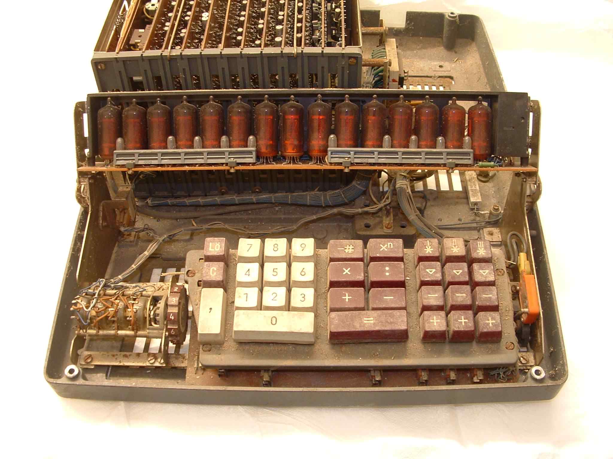
Its original condition!
Photos ©2011–
Click any photo for a larger image
And now refurbished
S#105669 - Technical Description
All images ©www.soemtron.org 2007–
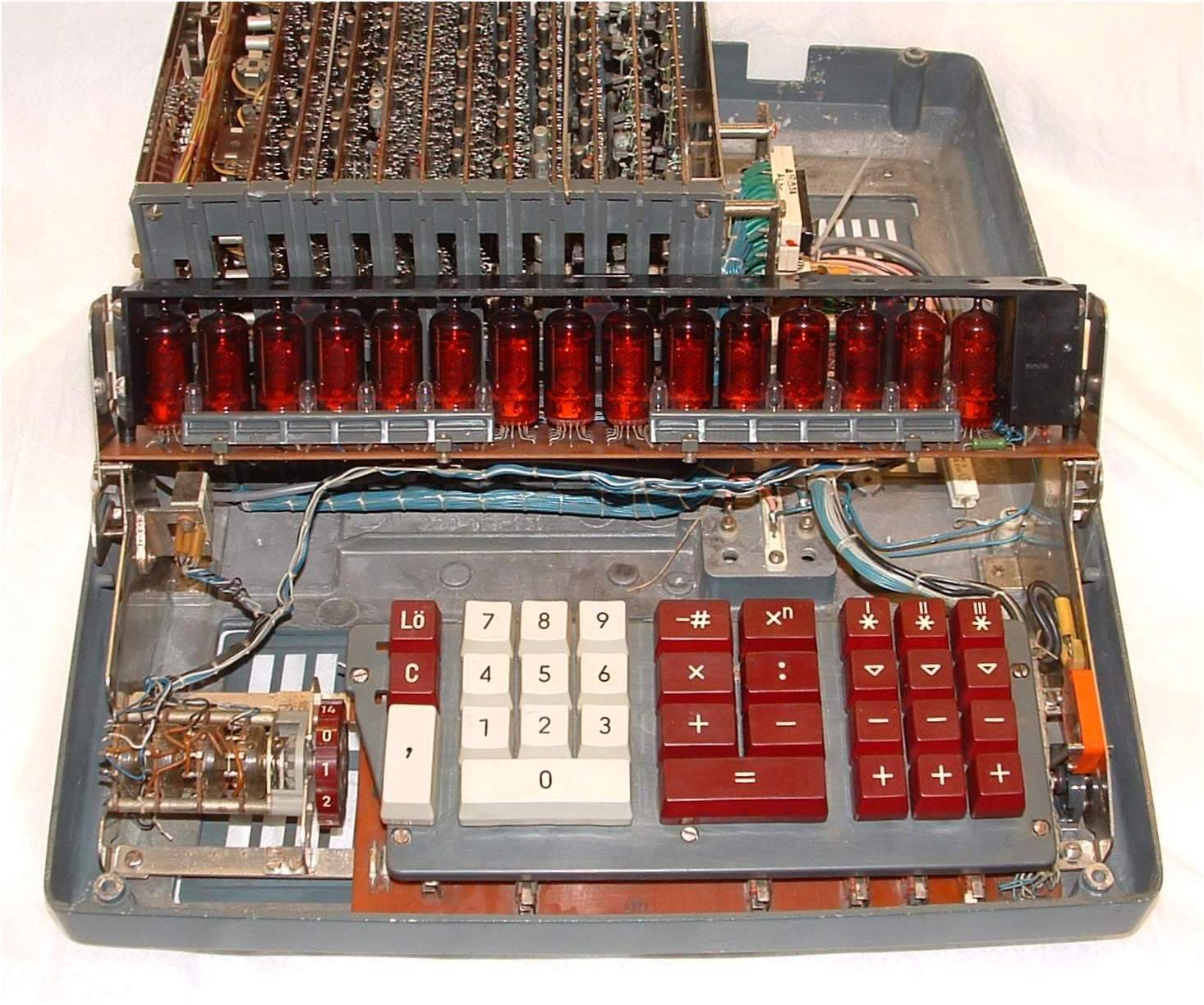
This Soemtron ETR220, our very first, was received in 2007 as an old piece of scrap equipment from Prague in the Czech Republic, after a Google search for "core memory" during some on–line research into the PDP–7 range of computers manufactured by the now defunct Digital Equipment Corporation. The unit duly arrived, but it was found to be in a very poor state, dirty, rusty and missing its power supply and top covers (see the top picture). It has a serial number of 105669, which we believe places it roughly two thirds through the production run of the Soemtron ETR22x series. This is reasonably backed up by the date codes found on the boards of between 17/73 to 22/73, presuming this date code is actually week and year, along with a rough calculation that puts serial number 105669 as being around week 18 of 1973. The base panels of the Soemtron ETR220 and 222 all seem to be the same, so we think the serial numbers were assigned to the bases before the machines were actually assembled, this theory seems to fit with the serial numbers and date codes of the machines we have, although admittedly this is a rather tenuous assumption!
Circuit and logic diagrams of this Soemtron ETR220, can be found on the Downloads page, or with each technical description below.
Power supply – circuit
The power supply is a fairly conventional series regulated unit, with outputs of –12V for the logic, +12V bias, and +13.5V for the core memory circuits and drivers. A fourth supply provides approximately +180Vdc for the display nixies. This display potential is actually split into +/- 90V DC rails. Using the standard continental mains input connector for the time, the power supply has an internal input voltage selector for 110, 127, 220 and 240V AC. Our original Soemtron ETR220 is missing its power supply so initially we were unable to derive a circuit diagram, but now with three other Soemtrons in our possession, another ETR220, a 222 and a rare 224, all having their power supplies intact, we have working samples to design a replacement power supply from.
| Lö | 7 | 8 | 9 | -# | Xn | I ✶ | II ✶ | III ✶ | |||
| C | 4 | 5 | 6 | x | : | ∇ | ∇ | ∇ | |||
| , | 1 | 2 | 3 | + | - | - | - | - | |||
| 0 | = | + | + | + | |||||||
Keyboard – circuit
The ETR220 keyboard consists of 31, microswitches capped with Red keys for control and functions, and White keys for numeric entry (see photo above), arranged in 4 logical groups thus -
- Clearing and decimal point keys - Master Clear Lö , Clear entry C and decimal point ,
- Numeric keys - 0-9 , arranged in the normal order as seen on modern computers and calculators.
- Arithmetic functions - Negate number -# , Raise to power Xn , Multiply X , Divide : , Add + , Subtract - and Result =
- Register controls - for registers I , II , III - Recall with clear ✶ , Recall ∇ , Subtract - and Add +
All signals from the keyboard go through a 32 plug/socket arrangement (PL17/SK17 on the drawings), to the backplane PCB where they are routed to Boards 11, display Anode drivers and 12, display Cathode drivers, for encoding in diode matrices. The Numeric keys 0-9 , clear entry C and decimal point , are routed to Board 12 for encoding, with a separate signal for the Master Clear key Lö going to the core store. See the Board 12 technical description below for logic and circuit diagrams. Note that the diode encoding matrix does not include diodes for all of the keys pressed, presumably to save on components, and that the codes are encoded by some of the keys acting directly on the diode matrix outputs. All of the other remaining keys are routed to Board 11 for encoding into five control signal lines for the three memory registers and functions. See the Board 11 technical description below for logic and circuit diagrams. As per the numeric encoding scheme, some of the keys act directly on the encoding matrix outputs.
The PCB is marked 05-220–1097-3b.
Display – circuit
The display consists of 15, Z570M Nixie tubes, a power "ON" neon, "negative" result lamp and 10 fixed position decimal point lamps. Each Nixie tube displays the numbers 0-9 in 13mm (0.51") high digits using a supply of 180Vdc at approximately 2mA. Each digit is a shaped metallic cathode of the required numeric shape and is commoned onto a multiplexed signal buss derived from Board 12, the display Cathode driver board. Each numerical digit has its own individual inverter driver on board 12 with a slight difference for the "0" digit due to the Display decimal point logic on Board 4 used during a numerical entry.
Each Nixie tube anode is separately driven from Board 11, the display Anode driver board via fifteen individual drivers, whose control signals are again derived from a multiplexed data buss. The ten Decimal Point lamps are directly switched from the last wafer of the front panel decimal point selection switch via a short cable loom and interconnecting 13pin plug and socket (PL13/SK17 on the drawings). The other three wafers of the decimal point selection switch encode eight signal lines for the main calculator control logic.
Board 1 – Core store, read amplifiers and digit drives 2–4 – circuit - logic
Board 1 contains the remaining display digit drivers for the 2, 3 and 4 digits in any of the fifteen digit positions of the display. Four read amplifiers HV1, 2, 4 and 8 are also on this board, wired directly to the read wire connections in each plane, they convert the EMF seen on a plane's read wire from the resulting polarity reversal of a core during a read operation. Two more core memory drivers are on this board, BL2 and BL4, which perform the "blocking" or inhibit functions for core planes 2 and 4, bits 2 and 4 of a BCD 1248 word.
- 3 input AND gates K3, K4, K5 generate signals DGDRV2 , DGDRV3 , DGDRV4 .
The PCB is date coded MAY 73, marked ETR220 on the component side, and 3033 05-220-7001-0 0e on the solder side. It appears that this board was used across the whole range of Soemtron ETR22x electronic calculators.
Board 2 – Core memory drivers, Read, Write and Inhibit decoding – circuit - logic
This board contains twenty of the twenty two memory drivers need to operate the core memory of a Soemtron ETR220. Each driver consists of a decoding logic gate, pulse amplifier, isolation transformer and driver transistor which then activate a corresponding wire in the core matrix according to the required function.
A 4uS monostable on the board generates timing signals T and T which are fed to all the driver input logic gates to ensure the correct pulse widths of the appropriate signals when applied to the core matrix. Each driver has a 3 or 4 input AND gate to decode that drivers function which cover Read, Write, Register addressing (MD, MR, AC0, AC1, AC2, AC3) and Inhibit actions.
The PCB is date coded 22/73, marked 4638 05-224-7002-5c on the solder side. This PCB's numbering therefore has this board being originally designed for an ETR224!
Board 3 – Arithmetic unit A Register, digit drives 5–9 – circuit - logic
Board 3 contains four flip–flops forming the "A" register (Ausgabe or output? result) of the Arithmetic unit and again are BCD encoded A1 , A2 , A4 , A8 and their complements A1 , A2 , A4 , A8 . The A register is closely coupled to the E register forming the Arithmetic unit of the machine.
The board also has five logic gates for decoding the digit signals for the 5, 6, 7, 8 and 9 digits in the display, and the decoding logic for the "C" buss, C1, C2, C4 and C8, part of the arithmetic logic unit.
- A 2 input AND gate K44 and four 3 input AND gates, K45, K46, K47, K48 generate the display signals DGDRV9 , DGDRV8 , DGDRV7 , DGDRV6 , DGDRV5 .
- Four AND–OR–Invert groups generate the signals C1 (K29, D1, N4), C2 (K33, D2, N3), C4 (K37, K43, D3, N6), C8 (K41, K43, D4, N8)
The PCB is date coded 22/73, marked 05-220-7003-5 0e and on the component side, and 3035 05-220-7003-5e on the solder side.
Board 4 – Arithmetic unit E Register, Carry latch and digit drives 0/1 – circuit - logic
Board 4 contains five flip–flops constructed from pairs of cross coupled PNP transistors with associated control gating, signal buffering and pulse circuitry. Four of these flip–flops are the "E" register (Eingang or input?) used to store BCD encoded numbers as E1 , E2 , E4 , E8 and their complements E1 , E2 , E4 , E8 , during numeric entry. The E register in concert with Board 3, the A register, forms the main arithmetic unit during calculations and data manipulation, with E register being used for bit carry operations as data bytes are fed to the A register. The fifth flip–flop is the arithmetic units byte "Carry" function labelled on the logic diagrams as UBER for "Ubertrag" or carry.
- E1/E8 - Numeric code during entry, Arithmetic unit.
- UBER - Arithmetic unit carry.
Decoding logic for the special "barred zero Ø" or "zero one" digit used to represent a decimal point in the display during a numerical entry is also on this board along with other display and control related logic.
- A 4 input AND gate K49 with inverter N43 generates signal E .
- A 3 input AND gate K28 generates signal K(LESVERV) .
- A 2 input AND gate K52 with inverter N12 generates signal G1 .
- A 2 input AND gate K63 with inverter N20 generates signal Z+E8 .
- A 6 input AND–OR group consisting of gate K57 and K62 with OR gate D6 generates the display signal DGDRV1 .
- A 5 input AND–OR–Invert group consisting of gate K56 and K59 and a signal from K57 above with OR gate D6 and inverters N17 and N18 signals X and X .
- A 4 input AND–OR–Invert group consisting of gate K53 with OR gate D8 and inverters N16 generates the display signal DGDRV0 .
The PCB is date coded 17/73, marked 05-220-7004-3 0h on the component side, and 05-220-7004-3 0i on the solder side.
Board 5 – V, SCHREIB, S1 function latches and 25Khz clock – circuit - logic
Board 5 contains three latches and various AND–OR gates similar to Board 6, it also contains the 25KhZ system clock generator and master system clock flip–flop. The function latches are labelled V, SCHREIB and S1 on the logic diagram. The function of V and S1 are not determined yet but SCHREIB is WRITE in English.
- V - (function not determined).
- S1 - (function not determined).
- SCHREIB - Read / Write flipflop.
There are eight gate groupings on board 5, three AND–OR–Invert, one AND-Invert, one OR-Invert and three AND.
- A 14 input AND–OR–Invert group consisting of AND gates K81, K82, K83 feeding OR gate D11 and then inverter N29 to generate signal MRS .
- A 14 input AND–OR–Invert group consisting of AND gates K85, K86, K87, K88 feeding OR gate D14 and then inverter N34 to generate signal HV .
- A 10 input AND–OR–Invert group consisting of AND gates K75, K76, K77 feeding OR gate D10 and then inverters N23 and N24 to generate signals RU and RU .
- A 5 input OR gate D13 feeding inverter N36 to generate signal Z which also feed one input of the 10 input group above and the 5 input AND below.
- A 5 input AND gate K91 generating signal K(ZDIV) which also feed one input of the 10 input group above.
- A 3 input AND gate K84 feeding inverter N32 and then inverter N33 to generate signal VLS .
- A 3 input AND gate K90 generating signal K90 .
- A 3 input AND gate K73 generating signal K(LESXUF) .
The PCB is date coded 21/73, marked 05-220-7005 1g on the component side, and 3037 05-220-7005–1h on the solder side.
Board 6 – Control gating – circuit - logic
Board 6 contains six major AND–OR–Invert gate groupings whose functions have not yet been determined. In all cases between one and eight multiple input AND gates feed a corresponding OR gate followed by one or more inverter buffers deriving the OR and NOR functions, one gate has multiple buffered outputs.
- 19 input AND–OR–Invert group consisting of AND gates K111, K113, K114, K115, K116 feeding OR gate D19 and inverters N46, N47 and N48. Generates signals ADD , ADD1 and SUB .
- 22 input AND–OR–Invert group consisting of AND gates K92, K93, K94, K95, K96, K97, K100 feeding OR gate D15 and inverter N38. Generates signal MRS .
- 38 input AND–OR–Invert group consisting of AND gates K101, K102, K103, K104, K105, K106, K107, K108 feeding OR gate D17. Generates signal MDS .
- 35 input AND–OR–Invert group consisting of AND gates K117, K118, K119, K120, K121, K122, K123, K124, feeding OR gate D21 and then inverter N43. The signal generated is fed to gates D22, D23 below.
- 9 input AND–OR–Invert group consisting of AND gates K127, K128, K129, K130, K131 feeding OR gate D22. Generates the signal AC0 .
- 2 input AND gates K125 and K126 feed 5 input OR gate D23 and then inverter N44 to generate the signal AC.
The PCB is date coded 21/73, marked 05-220-7006-8 0g on the component side, and 3038 05-220-7006-8 0e on the solder side.
Board 7 – B1–4, VOR and R function latches – circuit - logic
Board 7 contains six flip–flops constructed from pairs of cross coupled PNP transistors with associated control gating, signal buffering and pulse circuitry. The flip–flops are labelled B1–4, VOR and R on the logic diagram and appear to be used for the following functions - Add, Subtract, Multiply, Divide, Equality and raise to power functions and two as yet undetermined functions.
- B1 - Stores a pressed Add + or Subtract - key during entry.
- B2 - Stores the pressed Multiply X key during entry.
- B3 - Stores the pressed Divide : key during entry.
- B4 - Stores a pressed = or Xn key during entry.
- VOR - (function not determined, VOR is "before" or "in front of").
- R - (function not determined).
There are eleven gates of varying complexity ranging from single diodes to a four input AND-NOR gate, the functions of some of these gates are yet to be determined.
- K132 - 2 input AND, generates signal K(RFU) .
- K133 - 5 input AND, resets flip–flop B3 (Raise to power or Multiply).
- K134 - 3 input AND, resets flip–flop B4 (Divide).
- K135 - 4 input AND for inverter pair V567, signal DIV .
- K136 - 4 input AND to inverters N52 and N53, signals MUL and MUL .
- K137 - 4 input AND to inverters N55 and N56 for signal EING .
- K138, D26 - 3 input AND–OR input to inverter N54, signal G2 .
- K139 - 3 input AND, generates signal K(F1B4F) .
- K140 - 3 input AND, resets flip–flop B1 (Add / subtract).
- K142 - 3 input AND, resets flip–flop R (undetermined function).
- D24 - OR input for inverter N51, signal EING2 .
The PCB is date coded 22/73, marked 05-220-7007-6 0g on the component side, and 3039 05-220-7007-6 0g on the solder side.
Board 8 – F1, F3, VER and MZ function latches – circuit - logic
This board contains four flip–flops constructed in similar manner to the other boards. Flip–flop MZ is the Negative indicator flag driving the display negative lamp directly using a driver transistor on this board. The remaining three flip–flops on this board are unnumbered on the board but are listed as F1, F3 and VER in the German logic diagrams, their functions are yet to be determined.
- F1 - (function not determined).
- F3 - Cycles after Clear entry or +/- with Clear entry.
- VER - (function not determined).
- MZ - Negative result indicator.
There are a further two AND gates currently all of undetermined function, K152 and K111 which is split between this board and board 6.
- K152 - 4 input AND, generates signal K(RS16).
- K111 - 2 (4) input AND, generates signal K(RB4MZ) .
The PCB is date coded 22/73, marked 05-220-7008-4 0f on the component side, and 3040 05-220-7008-4 0f on the solder side.
Board 9 – F2, F4, F5, F6 function latches, including register addressing – circuit - logic
Board 9 contains four flip–flops, again constructed from pairs of cross coupled PNP transistors with associated control gating, signal buffering and pulse circuitry. On the logic diagram they are labelled F2, F4, F5 and F6. Part of board 9's function in this Soemtron ETR220 has been ascertained as the two bit binary addressing for the three temporary memory registers (AC1, AC2 and AC3) using flip–flops F4 and F5, F5 having the test point label MP10 for bit two of the addressing scheme. Of the remaining two flip–flops, F2 and F6, are unmarked on this board but their functions seem to be temporary flags for the Add, Subtract, Multiply, Divide, -# and Xn functions.
- F2 - Active during Add, Subtract and Divide.
- F4 - Temporary register address bit 1.
- F5 - Temporary register address bit 2.
- F6 - Active during Multiply, Divide, -# and Xn.
This board also contains the keyboard de–bounce and delay circuitry derived from signals NUMKEYS and FNCTKEY to generate the signal KEYPRESS , (" xxx " denotes a negated signal). Master reset circuitry for all of the flip–flops in the machine is derived directly from the Lö key via the signal KBD(LO1) which is then distributed to other boards in the card rack. There are a further three AND gates and an 18 input AND-NOR gate.
- K169 - 3 input AND, generates signal K(S16DIVF1) .
- K161 - 4 input AND, generates signal CO .
- K162 - 2 input AND, generates signal K(MS) .
- K164 - 5 input AND, input for D25.
- K165 - 5 input AND, input for D25.
- K165 - 4 input AND, input for D25.
- K166 - 3 input AND, input for D25.
- D25 - 5 input OR, generates signal M.
The PCB is marked 05-220-7009-2 0e on the component side, and 3041 05-220-7009-2 0h on the solder side.
Board 10 – 5 bit address "Z" counter – circuit - logic
Board 10 contains five cascaded flip–flops connected as a five bit BCD counter. Each flip–flop is constructed from pairs of cross coupled PNP transistors with associated control gating and signal buffering and pulse circuitry. Its function is to generate a four bit BCD count (0–15) for the nixie display and a five bit count (0-31) for calculations.
Complex input gating to the Z counter determines the initial state and operating conditions of the Z counter during calculations, but for display purposes, the counter purely cycles through a repetitive 1 - 2 - 4 - 8 sequence deriving the signals for the multiplexed display anode drivers on Board 11. This dual use of the Z counter for both display multiplexing and calculations give the Soemtron ETR220 and 222 calculators their distinctive "ripple" effect in the display during larger calculations, especially multiplication and division. Further gating or another counter would have meant a cleaner display but at the expense of more logic and components, increasing costs.
The individual flip–flops on this board have test points labelled MPx, with MP being "MessPunt" in German. The flip–flops are numbered Z1, Z2, Z4, Z8, Z16 with test points MP9, MP17, MP42, MP56, MP58, and they generate signals Z1 - Z1 , Z2 - Z2 , Z4 - Z4 , Z8 - Z8 , Z16 , S16 and S16 .
The PCB is date coded 21/73, and marked 3042 05-220-7010-7 f on the solder side.
Board 11 – Display Anode Drivers, function key encoding – circuit - logic
15, NPN transistor pairs with addressing matrix and signal conditioning. Each Nixie tube Anode is controlled by a four input diode gate decoding eight BCD control signals (Z1, Z2, Z4, Z8 and their complements) from the Z counter on board 10, to successively enable each tube in turn for a set period, to coincide with data signals on the display data buss. The NPN transistors are type BS02. Board 11 contains the remaining keyboard encoding sections for the function and register key groups, see the board 11 logic and circuit diagrams for the encoding scheme.
Pressing any of the function keys generates a strobe signal ANYKEY , with any of the following signals –
- Pressing any key of the three sets of register keys generates a two bit binary encoded register address SELREG1 and SELREG2 .
- The four register functions + - ✶ ∇ generate KY(ADD) , KY(SUB) and ANYRGX (recall with clear), with all three signals absent being the register function ∇ or RECALL .
- The remaining six arithmetical functions + - X : = -# Xn are also encoded within the matrix on board 11 into KY(ADD) , KY(SUB) , KY(MUL) , KY(DIV) , KY(EQU) , KY(NEG) and KY(RAISE) respectively.
The PCB is date coded 20/73, and is marked 3043 05-220-7011-5 0g on the solder side.
Board 12 – Display Cathode Drivers, numeric key encoding – circuit - logic
14, PNP/NPN transistor pairs driving a common cathode multiplexed display buss from an internal data buss. Each pair consists of a PNP transistor inverting and conditioning the data buss signals, feeding an NPN transistor driving the commoned display cathodes, each with an output clamp diode. However the driver for the "1" cathode buss is quite different in that it does not have the inversion and conditioning PNP transistor stage, but drives the "1" cathode buss directly with a solitary NPN transistor. This difference is due to the decoding logic of the "0" and "1" digits and the ability to display both digits simultaneously as a "barred zero Ø" to represent the current decimal point position during entry.
Board 12 also contains that part of the keyboard encoding circuitry concerned with the 0-9 numeric keys (BCD 0-9), the clear entry C (BCD 15) key, and decimal point , (BCD 12) key. The numeric keys 0-9 and the decimal point , are encoded into a 4bit BCD word (signals NUM1 , NUM2 , NUM4 , NUM8 ) with a separate signal line for the clear entry C key (signal KYCLER ). A master reset key Lö acts directly on the Core Store (Board 1) via the signal LöSPE to clear the AC0, MR and MD registers, the three temporary storage registers AC1, AC2 and AC3 are not cleared by the Lö key.
The PCB is date coded 22/73, marked 05-220-7012-3 0h on the component side and 3044 05-220-7012-3 0f on the solder side. In this particular Soemtron ETR220 driver board the NPN transistors are type BS02 and the PNP transistors are type GS121.
Site design ©2007– soemtron.org - privacy -