The Soemtron ETR220 Calculator
Skip to navigationLatest news (September 2019) - Wolfgang Robel's video and ETR220 pages.
 |
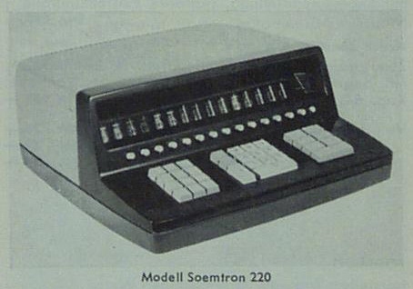
 Soemtron ETR220 Click image for a larger version ©2007 Serge Devidts |
Manufactured from 1966 to 1977 by V.E.B.[1] Büromaschinenwerk[2] Sömmerda, 155,142[3] Soemtron ETR220 desktop calculators[4] were built during the eleven year production run from 1966 to 1977. With six functions[5], the processing logic of the Soemtron ETR220 calculator is all transistorised, consisting mostly of pairs of PNP Germanium transistors with a few resistors, capacitors and diodes coupled as Flip Flops (latches), and further sets of diodes for gating functions.
The keyboard is large and cumbersome, non-multiplexed, utilising large microswitches (thought to be V23's[6]) with external supplementary return springs for the keys themselves. The unit has three memories for intermediate calculations, each with their own set of Recall/Clear, Recall, Add and Subtract keys. There is also a "C" key which clears the current entry and a "Lö" key which clears everything excepting the three operand stores. The 15 digit display of Z570M "Nixie" tubes is multiplexed and uses a supply of around 180Vdc.
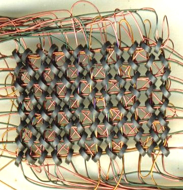 Soemtron ETR222 core store ©2007 www.robotrontechnik.de Click image for a larger version | |
The Soemtron ETR220 has a four plane (1248 BCD) "Ferritkernspeichern"[7] or magnetic core memory consisting of 6 x 16 digit registers, a total of 384 bits or 48 bytes, showing the age of the machine from a time when magnetic core memory was THE "modern" technology before the advent of multi-megabyte semiconductor RAM. Over the eleven year production run for the ETR220, 7.4Mb of magnetic core storage or nearly 60,000,000 miniature ferrite cores were hand threaded onto many thousands of kilometres of copper wire.
The power supply and card cage construction of very early model Soemtron ETR220's is different to later models in production. Confirmed by retired engineers from the Sömmerda factory in a visit to Germany, very early machines had a reversed board order, I.E. board 1 (memory) was in the middle of the machine close to the power supply, with board 12 (display driver) being on the outer left hand side. The power supply was also slightly different, as the main series pass regulator transistor was internally mounted on a heat sink panel rather than on the base of the machine as in later models. It would appear that the reasoning for these changes stemmed mainly from the sensitivity of the Ferrite core memory to temperature and magnetic fluctuations caused by the power supply transformer. Moving the regulator transistor to the base gave a simpler assembly and better operation as it moved a heat source to the bottom of the case away from the interior of the unit. See the 220 Gallery for photos of Philipp Maier's early reversed build Soemtron ETR220 S#27027 from around 1967-68.
|
 Early model Soemtron ETR220 with individual decimal point selection switches Click image for a larger version ©2009 Serge Devidts |
Decimal point selection is by a 12 position thumb-wheel switch to the left of the main numeric keypad, which is also indicated on the display by small incandescent lamps in between most Nixie tubes giving the impression of a comma, a range of decimal point selection signals are directed back to the logic circuits for use during calculations. This makes the Soemtron ETR220 a "fixed point" machine rather than the usual "floating point" form found on modern calculators. Very early versions of the ETR220 did not have the thumb-wheel switch but instead used a row of illuminated switches on the front panel just below the display window (picture right).
Circuit and logic diagrams of the Soemtron ETR220 can be found on the Downloads page, or with each technical description below. Our original Soemtron ETR220, missing its case and the vital power supply has a serial number of 105669, which we believe places it roughly two thirds through the production run of the Soemtron 22x series. This is reasonably backed up by the date codes found on the boards of between 17/73 to 22/73. We calculate serial number 105669 as being week 18 of 1973, presuming this date code is actually week and year. Our second, complete, but damaged ETR220 is serial number 54555, so we think should have been made in about week 41 of 1969, we'll have a look and let you know! The base panels of the Soemtron ETR220 and 222 all seem to be the same, so we think the serial numbers were assigned to the bases before the machines were actually assembled, this theory seems to fit with the serial numbers and date codes of the machines we have, although admittedly this is a rather tenuous assumption!
The re-use of circuitry and clever logic design of the Soemtron ETR220 (carried over to the 224 and then the 222 models) produced a first generation electronic calculator that as far as possible gave maximum functionality with the minimum component count. Microprocessors were not yet readily commercially available at a time when more functionality = more complexity = more components = more cost. Design re-use was the norm, and this might have given the end result some "quirkiness", for example - dual use of the Z counter for both display multiplexing and during operation give the Soemtron ETR220 and 222 calculators their distinctive "ripple" effect in the display during larger calculations, especially multiplication and division. Further gating or another counter would have meant a cleaner display but at the expense of more logic and components, thereby increasing costs. A lesson probably lost in modern designs where the maxim of - throw more logic, or more software, at a problem - is the norm - more is not always best.
In 1967 the Soemtron ETR220 was priced at £485.0.0d (about £7,200 at 2015 values!) and was described as - "the new Soemtron ETR220 . . . . in fact one of the least expensive machines on the market at this specification, delivery could be effected within 14 days".

If you have any further historical information, circuits, drawings, photographs, data or manuals about the Soemtron ETR220, 221, 222 and 224 or their manufacture, test equipment (Prüfgeräte) or you just know more about the Soemtron companies in general then please let us know, contact us.
September 2019 - In an email from Wolfgang Robel, another of our contributors, Wolfgang has let us know of a video he has posted on YouTube entitled "Rechnen mit Transistoren und Nixies - Die Soemtron ETR220" (Computing with transistors and nixies - the Soemtron ETR220). This 26 minute video delves into the innards of the "Retro Calculating" scene in what is one of the earliest Nixie calculators in the days before integrated circuits and processor chips - the Soemtron ETR220. (Wolfgang's website is in German).
- Wolfgang also lists three further links for the Soemtron ETR220 -
- Soemtron core store: http://www.wolfgangrobel.de/museum/soemtron.htm
- Soemtron repaired : http://www.wolfgangrobel.de/museum/etr220.htm
- Soemtron - how does that work: http://www.wolfgangrobel.de/museum/etr220.htm#upd[top]
August 2011 - An email from another of our contributors Rocco Thiel has turned up two Soemtron brochures from the 1960's, one for the ETR220 and one for the ETR221. The ETR221 brochure is especially welcome as we thought that publicity information about this machine did not exist. The ETR220 brochure is available for download; the 221 brochure can also be viewed.
September 2010 - An email from Bernard Green has passed on some ETR220 sales literature he received from VDI Verlag, Düsseldorf. They have forwarded an extract from the VDI-Z Association of German Engineers magazine, volume 108 (July 1966), page 944. In the very small entry for the ETR220 it states (translated) -
"Desk calculator Soemtron ETR220 - The electronic desk calculator Soemtron ETR220 has three memories with Rückübertragungseinrichtung (recall facility?). Its average computing time is 0,5s and the capacity of the computer input and output is 15 digits. The electronics assembly is in one separate housing. (Office machines export GmbH, Berlin)". The 221 page can be viewed (©2010 VDI Verlag, Düsseldorf).
| 1 | Wikipedia entry for V.E.B. = Volks Eigener Betrieb, or Peoples Owned Company | V.E.B.[top] |
| 2 | Büromaschinenwerk. | Office Machine Works.[top] |
| 3 | ETR220 production of 155,142 during 1966-1977 | Page 389 "BWS Sömmerda", by Annegret Schüle ISBN 39-8039-311-9, ©1995 Desotron Erfurt.[top] |
| 4 | Desk top calculator Calculator. |
Tischrechner. Rechenmaschine.[top] |
| 5 | Functions | Negate number, Raise to power, Add, Subtract, Multiply, Divide.[top] |
| 6 | V23 microswitch | Originally thought to be a V23 microswitch variant, the correct style is the ABB or Petercem, M & CM style switches (data sheets ABB, Petercem), but with right angle PCB pins. Data for these particular right angle PCB mount switches however, does not seem to be available even though they are from the M/CM range.[back] [top] |
| 7 | Ferritkernspeichern | Ferrite Core Memory.[back] [top] |
Site design ©2007- - privacy -