ETR222
S#74005
222 Gallery
Soemtron ETR222 Calculator
Skip to navigation |
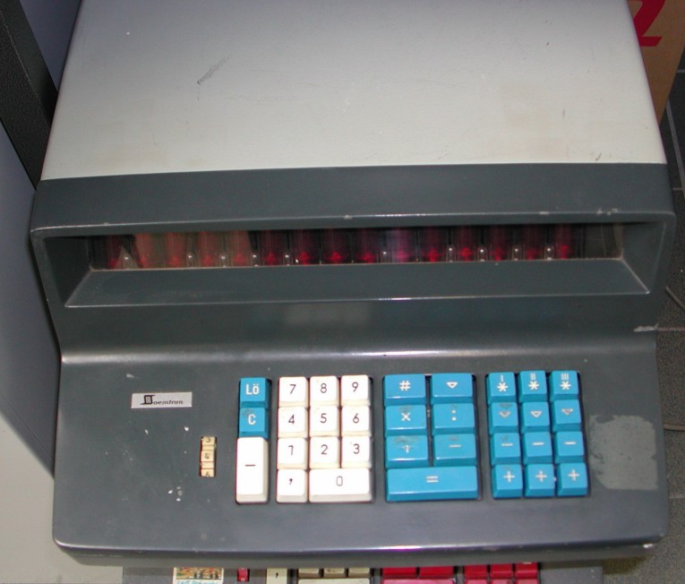 Soemtron ETR222 ©2007 Serge Devidts Click image for a larger version |
S#74005 - Technical Description
This ETR222, our third Soemtron calculator, is complete but it has a slightly damaged keyboard from a lifetime of use. It appears to be one of only six[1] Soemtron ETR222's existing that we know of from the original 3,203 units that were built. It has a serial number of 74005, which we believe places it roughly half way through the production run of the Soemtron ETR22x series, sometime in 1971 possibly about week eight or nine. The base panels of the Soemtron ETR220 and 222's all seem to be the same, so we think the serial numbers were assigned to the bases before the machines were actually built, this theory seems to fit with the serial numbers and date codes of the machines we have, although admittedly this is a rather tenuous assumption!
March 2021 - Reverse engineering our Soemtron ETR222 is just about complete and the results have confirmed that the ETR222 is in fact derived from the ETR224, not the ETR220 as we thought some while ago. Several of the main PCB's are labelled "224-" (the "4" is scratched out) and several "22 -", with several being at the same issue level as the corresponding PCB of the ETR224 board.
Power supply - circuit
The power supply is the same fairly conventional series regulated unit as fitted to the ETR220, with outputs of -12V for the logic, +12V bias, and +13.5V for the core memory circuits and drivers. A fourth supply provides approximately +180Vdc for the display nixies. This display potential is actually split into +/- 90V DC rails. Using the standard continental mains input connector for the time, the power supply has an internal input voltage selector for 110, 127, 220 and 240V AC.
Keyboard - circuit - logic
The keyboard layout of the ETR224 was copied for the Soemtron 222, but with the main differences to a standard ETR220 being -
- The sign or negate entry key (220 -# ) is moved from the central functional key group to the space below the Clear key C previously occupied on the ETR220 by the decimal point key , - which then
- moves to a new location under the numeric 1 key left of the now slightly smaller zero 0 key. The current decimal point position (overlaid 0 and 1 digits to show as a "barred" 0), is now not visible in the display during numeric input.
- The ETR220 "Raise to Power" function key Xn has been removed. For powers on an ETR222 the base number X is first keyed in, then for the exponent n, the multiplication key is pressed n-1 times, then the equals key once. This key position has become the "return constant" ∇ key.
- Lastly the key position on an ETR220 for the "sign or negate entry key" -# becomes the "Exchange operands" # key which swaps the contents of both operand registers.
| Lö | 7 | 8 | 9 | # | ∇ | I ✶ | II ✶ | III ✶ | |||
| C | 4 | 5 | 6 | x | : | ∇ | ∇ | ∇ | |||
| - | 1 | 2 | 3 | + | - | - | - | - | |||
| , | 0 | = | + | + | + | ||||||
The ETR222 keyboard consists of 32, microswitches with Blue keys for control and functions, and White keys for numeric entry (see photo above), arranged in 4 logical groups broadly similar to the ETR220 thus -
- Clear and sign keys - Clear Lö , Clear entry C and negate entry -
- Numeric keys - 0-9 , arranged in the normal order as seen on modern computers and calculators, and decimal point ,
- Arithmetic functions - exchange operands # , return constant ∇ , Multiply X , Divide : , Add + , Subtract - and Result =
- Register controls - for registers I , II , III - Recall with clear ✶ , Recall ∇ , Subtract - and Add +
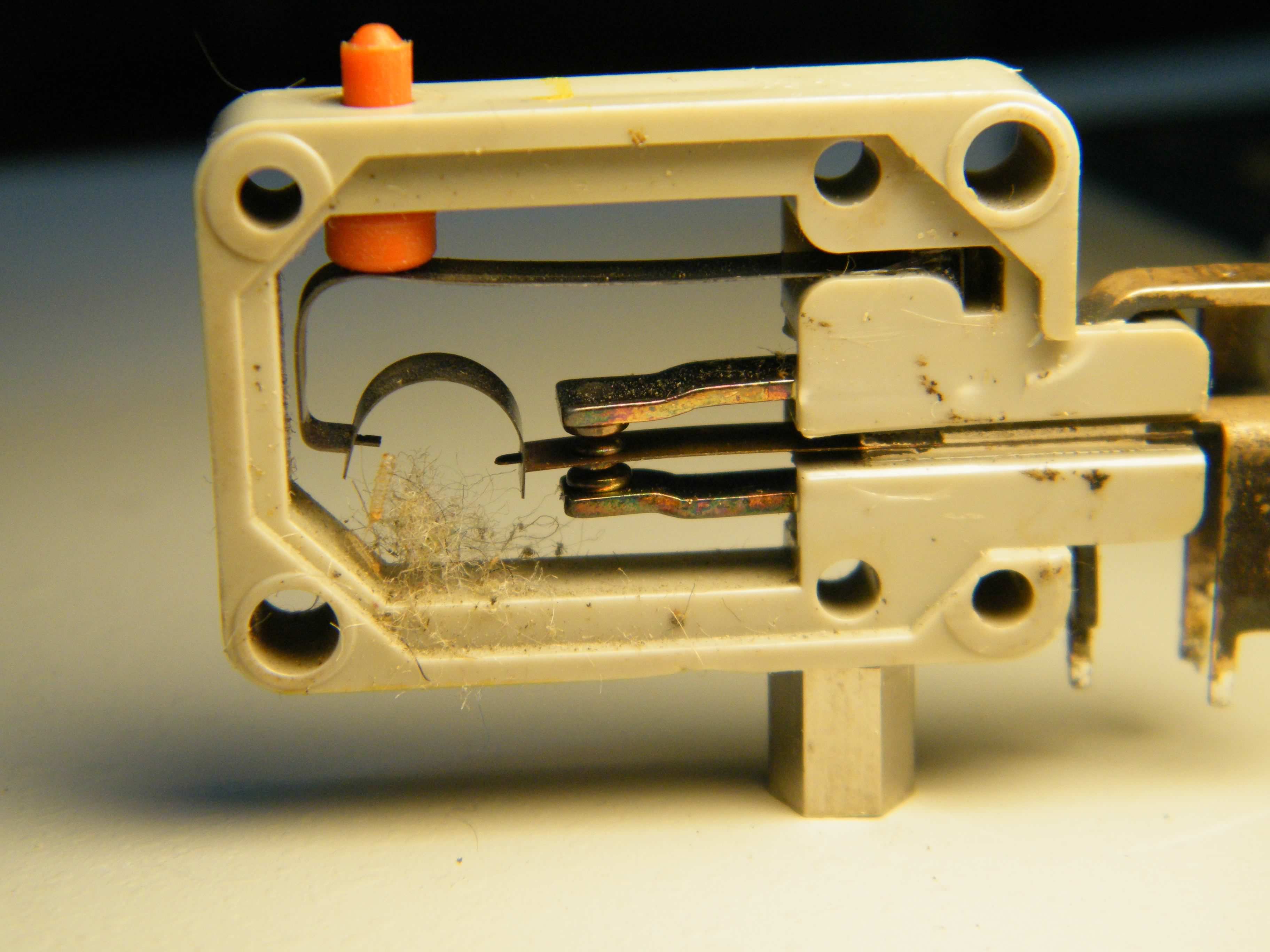 ©2018 www.soemtron.org Larval carcasses inside a keyboard switch (covers removed) Click image for a larger version | |
Whilst reverse engineering our ETR222 back to a circuit diagram, we found several of the keyboard micro-switches were not working on the common return line KBD(K), most were down to contact oxidisation of the normally open contact from years of not being used, however, one was found to have what looked like a couple of maggot like larval carcasses and fiber debris. How this wildlife debris got inside what effectively is a sealed switch we don't know but cleaning it out brought the switch back to operation. Long term oxidisation of switches can be "electrically" cleaned by passing a relatively high but limited current through them, something in the order of 300mA. This process somewhat resembles the old process of providing a "whetting" current for switch and relay contacts specifically to punch through contact oxidisation. Keyboard circuits within the Soemtron ETR series calculators typically only have 0.8mA flowing as a "whetting" current, not nearly enough to perform this function.
We have made up a small jig for this purpose but it does mean the switches must be removed from the keyboard assembly. The jig is configured to pass 300mA & 30V through the contacts, with a couple of LED's to show when the switch is working. Initially one or both of the contacts, usually the normally open, will not give a LED indication (from the oxidisation), subsequent repeated operation of the switch should bring it back to life within a few cycles and we have found this process to be quite effective. Switches that do not respond can also be manually cleaned with a contact cleaner, but you will need to carefully remove the clear side covers by prising off the side that has the heat welded location pins. With care the weld will snap easily and the cover removed, on replacing fix with a small amount of a clear super glue at the site of the original welds.
Display - circuit - logic
The display consists of 15, Z570M Nixie tubes, a power "ON" neon, "negative" result lamp and 10 fixed position decimal point lamps. Each Nixie tube displays the numbers 0-9 in 13mm (0.51") high digits using a supply of 180Vdc at approximately 2mA. Each digit is a shaped metallic cathode of the required numeric shape and is commoned onto a multiplexed signal buss, with each numerical digit having its own individual inverter driver.
The Anode for each Nixie tube is also separately driven via fifteen individual drivers, whose control signals are again derived from a multiplexed data buss. The ten Decimal Point lamps are directly switched from the last wafer of the front panel decimal point selection switch via a short cable loom and interconnecting 13pin plug and socket. The other three wafers of the decimal point selection switch encode eight signal lines for the main calculator control logic.
Board 1 - Core store, read amplifiers and digit drives 2-4 - circuit - logic
Board 1 contains the four read amplifiers HV1, 2, 4 and 8, wired directly to the read wire connections in each plane, they convert the EMF signal seen on a plane's read wire from the resulting polarity reversal of a core during a read operation. Two core memory drivers are also on this board, BL2 and BL4, which perform the "blocking" or inhibit functions for core planes 2 and 4 used for bits 2 and 4 of of each BCD (1248) word in memory.
- The board also contains 3 AND gates (2x 4 input and 1x 3 input) numbered K3, K4 and K5 which generate signals DGDRV2 , DGDRV2 , DGDRV4 from the A and C registers used by the cathode drivers on the under keyboard PCB, multiplexing the 2, 3 and 4 grids within each of the 15 display Nixies.
The PCB is marked ETR224 on the component side, and 3033- 220-317-001c on the solder side. It appears that this board was used across the whole range of Soemtron ETR22x electronic calculators.
Board 2 - Core memory drivers, Read, Write and Inhibit decoding - circuit - logic
This board contains twenty of the twenty two memory drivers need to operate the core memory of a Soemtron 222. Each driver consists of a decoding logic gate, pulse amplifier, isolation transformer and driver transistor which then activate a corresponding wire in the core matrix according to the required function.
A 4uS monostable on the board through inverters N1 and N2 generate timing signals T and T which are fed to all the driver input logic gates to ensure the correct pulse width and timing of the appropriate signals when applied to the core matrix. Each driver has a 3 or 4 input AND gate to decode that drivers function which covers Read, Write, Register addressing (MD, MR, AC0, AC1, AC2, AC3) and Inhibit actions.
The PCB is date coded 40/68 and marked 3034- 220-317-002d on the solder side.
Board 3 - B1-4, VOR and Unknown function latches - circuit - logic
The six flip-flops of board 3 contains are constructed from pairs of cross coupled PNP transistors with associated control gating, signal buffering and pulse circuitry. The flip-flops are labelled B1 , B2 , B3 , B4 , VOR and Unknown on the logic diagram and appear to be used for the following functions - Add, Subtract, Multiply, Divide, Equality and raise to power functions and two as yet undetermined functions.
- B1 - Stores a pressed + or Subtract - key during entry
- B2 - Stores the pressed Divide : key during entry
- B3 - Stores the pressed Multiply X key during entry
- B4 - Stores a pressed = or Xn key during entry
- VOR - Carry ? (function not determined, VOR is "before" or "in front of")
- Unknown - (function not determined)
There are fourteen gates of varying complexity ranging from single diodes to a four input AND-NOR gate, the functions of some of these gates are yet to be determined.
- K??? - 2 input AND, resets flip-flops B3 (Raise to power) and B4 (Divide)
- K??? - 2 input AND, resets flip-flop B1 (Add or Subtract)
- K??? - 2 input AND, resets flip-flop VOR (undetermined function)
- K??? - 3 input AND, resets flip-flops B3 (Raise to power) B4 (Divide)
- K??? - 3 input AND, resets flip-flop R (undetermined function)
- K??? - 3 input AND, generates signal K(MULF3V)
- K??? - 3 input AND, generates signal TMP-A8
- K137 - 3 input AND for inverters N55 and N56, signals K(ZS1R) , resetting the VOR , B3 and B4 flip-flops
- K??? - 4 input AND for inverter pair for inverters N?? and N??7, signal DIV
- K136 - 5 input AND K136 to inverters N52 and N53, signals MUL and MUL
- D24 - 3 input OR for inverter N??, signal D(DBLVORF2)
- D?? - 2 input OR for inverters N?? and N??, signals D(B3B4) and D(B3B4)
- D?? - 1 input OR from KBD(Lö1) to reset the A8 flip-flop on board ?
The PCB is date coded 25/69 and marked 3966- 22 -307-003d on the solder side.
Board 5 - 5 bit address "Z" counter - circuit - logic
Board 5 contains five cascaded flip-flops connected as a five bit BCD counter. Each flip-flop is constructed from pairs of cross coupled PNP transistors with associated control gating and signal buffering and pulse circuitry. Its function is to generate a four bit BCD count (0-15) for the nixie display and a five bit count (0-31) for calculations.
Complex input gating to the Z counter determines the initial state and operating conditions of the Z counter during calculations, but for display purposes, the counter purely cycles through a repetitive 1 - 2 - 4 - 8 sequence deriving the signals for the multiplexed display anode drivers on Board ?? the under keyboard display decoder board. This dual use of the Z counter for both display multiplexing and calculations give the Soemtron ETR220 and ETR222 calculators their distinctive "ripple" effect in the display during larger calculations, especially multiplication and division. Further gating or another counter would have meant a cleaner display but at the expense of more logic and components, increasing costs.
The flip-flops generate signals Z1, Z2 , Z4 , Z8 , Z16 and S16 with their complements - Z1 , Z2 , Z4 , Z8 , S16 .
- K63 - 2 input AND to inverter N20 for signal K(E8Z)
- K??? - 2 input AND for signal DRV2
- K??? - 3 input AND for signal DRV18
- K??? - 5 input AND for signal DRV15
The PCB is date coded 14/69 and marked 3965- 22 -307-004c on the solder side.
Board 5 - 25Khz clock, R, F6, undetermined functions, 14 drive signals - circuit - logic
Board 5 contains four latches and various AND-OR gates, it also contains the 25KhZ system clock generator. The function latches are labelled R , F6 with 2 as yet undetermined functions on the logic diagram..
- R - (function not determined)
- F6 - (function not determined)
- and two undetermined functions
There are six other gate groupings on board 5 along with six inverters.
- K196 - 5 input AND for inverter N29 to generate signal S16 . This then feeds K212, a 2 input AND with signal RU for inverter N?? to generate signal S16
- D13 - 5 input OR gate for inverter N36 to generate signal Z
- K??? - 2 input AND for signal K(Z16F2)
- K??? - 4 input AND for signal K(Z1Z2DIVZ4RUZ8)
- K??? - 3 input AND for inverter N?? to generate signal K(S16DBLF2)
- Inverter N37 to buffer the master clock generate signal S
The PCB is date coded 34/68 and marked 3960- 224-307-005a on the solder side.
Board 6 - Wheel position, M latch, undetermined function, various gating - circuit - logic
Board 5 contains six latches and various gates and inverters. Four of the flip-flops are connected in a 4-bit counter which on an ETR224 formed the print wheel position reference WCNTx and WCNTx . Its use in this ETR222 has been disabled so presumably the board is retained for the remaining latches and gating functions. The remaining flip-flops are for M and one other as yet undetermined function on the logic diagram..
- Four latches generate signals WCNT(1248) and WCNT(1248) , however they have been disabled by removing the transistors and their corresponding collector load resistors for each flip-flop, the position index clock input ( PCLK ) on the counter first stage has also been removed
- M - (function not determined)
- and one undetermined function
There are eight other gate groupings on board 6 along with nine inverters.
- K??? - 4 input AND with a 2 input OR subsection followed by two inverters N?? and N?? generate signal D(WCNT48VERPRT) and its complement D(WCNT48VERPRT) , however these two signals have been disabled to their OFF states by removing the AND input diode gating. The OR subsection inputs remain operational to generate the signal PRINT , in the ETR224 this started a one line print, in the ETR222 the use of this signal is yet to be determined
- K??? - a six input AND gate with two inverters N?? and N?? generate signal TMP-B22 a temporary signal whilst we work out the correct one (this might be - K(VRRDF2DBLUBRZ1)
- K??? - Five input AND gate generating signal K(UBERVERDBLF2RCLK) , one input ( PCLK ) to this gate has been disabled by removing the diode
- K??? - 3 input AND for signal DRV1
- K??? - 2 input AND for signal K(Z8VER)
- K??? - 3 input AND for signal K(UBERWCNT842) , this gate is split between board 6 and board 11
- K??? - 4 input AND for inverter N?? (not fitted) to generate signal K(UBRS16VRDBL)
- D?? - eight input OR with 8 K??? two input ANDs to form an eight bit comparator between the Wheel counter signals on this board and the A register on board 7. A subsequent three input AND gate and two inverters originate signals PCLK and, WHLSTRB . Two of the three inputs are disabled and the second inverter does not have the transistor and collector load so the two signals are effectively disabled
Lastly a resistor capacitor network for the keyboard CLEAR key, located here presumably it was either left off the keyboard decoding circuitry or there was limited space.
The PCB is date coded 35/68 and marked 3969- 224-307-006b on the solder side.
Board 7 - Arithmetic unit A Register, digit drives 5-9 - circuit - logic
Board 7 contains four flip-flops forming the "A" register (Ausgabe or output? result) of the Arithmetic which is BCD encoded as A1 , A2 , A4 , A8 and their complements A1 , A2 , A4 , A8 . The A register is closely coupled to the E register on board 8, forming the Arithmetic unit of the machine, multiple SET inputs to each bit of the A register are disabled when used in the ETR222.
Four AND-OR-Invert groups decode and generate the signals for the "C" buss, C1 , C2 , C4 and C8 , also part of the arithmetic logic unit.
- K29, D1, N4 - for C1
- K33, D2, N3 - for C2
- K37, D3, N6 - for C4
- K41, K43, D4, N8 - for C8. One input of K43, K(UBRS16VRDBL) is disabled
The PCB is date coded 33/68 and marked 3959- 224-307-007a on the solder side.
Board 8 - Arithmetic unit E Register, Carry latch and digit drives 0/1 - circuit - logic
Board 8 contains five flip-flops constructed from pairs of cross coupled PNP transistors with associated control gating, signal buffering and pulse circuitry. Four of these flip-flops are the "E" register (Eingang or input?) used to store BCD encoded numbers as E1 , E2 , E4 , E8 and their complements E1 , E2 , E4 , E8 , during numeric entry. The E register in concert with Board 7, the A register, forms the main arithmetic processing unit during calculations and data manipulation, with the E register being used for bit carry operations as data bytes are fed to the A register. The fifth flip-flop is function UV the function of which is yet to be determined.
Decoding logic for the special "barred zero Ø" or "zero one" digit used to represent a decimal point in the display during a numerical entry is also on this board along with other display and control related logic.
- K49 - four input AND gate with inverter N43 generates signal E
- K28 - three input AND gate generates signal K(LESVERV)
- K52 - input AND gate with inverter N12 generates signal G1
- K63 - two input AND gate with inverter N20 generates signal Z+E8
- K57, K62 D6 - six input AND-OR group consisting of gate generates the display signal DGDRV1
- K56, K59 - five input AND-OR-Invert group with a signal from K57 feed inverters N17 and N18 signals X and X
- K53, D8 - four input AND-OR-Invert group and inverter N16 generates the display signal DGDRV0
The PCB is date coded 40/69 and marked 3952- 224-307-008a on the solder side.
Board 9 - READ/WRITE, S1, V, miscellaneous gating - circuit - logic
Board 9 contains three flip-flops constructed in the usual manner from pairs of cross coupled PNP transistors with associated control gating, signal buffering and pulse circuitry. The READ/WRITE (Les - Schreib) flip-flop controls the operation of the core memory planes on Board 1 via the drivers on Board 2. The functions of flip-flops S1 and V are yet to be determined. There are five AND-OR-Invert gate groupings whose functions have not yet been determined in the overall logic flow of the ETR222. In all cases between two and eight multiple input AND gates feed a corresponding OR gate followed by one or more inverter buffers deriving the AND-OR and NOR functions.
- A 31 input AND-OR-Invert group consisting of eight AND gates (all K??) feeding OR gate D?? and inverter N?? to generate signal TMP-B38
- A 14 input AND-OR-Invert group consisting of AND gates K85, K??(86?), K87 feeding OR gate D14 and then inverter N34 to generate signal HV
- A 10 input AND-OR-Invert group consisting of AND gates K75, K76, K77 feeding OR gate D10 and then inverters N23 and N24 to generate signals RU and RU
- A 4 input AND-OR-Invert group consisting of AND gates K??, K?? feeding OR gate D?? and inverter N?? to generate signal D((RM)(F4MUL))
- A 4 input AND-OR-Invert group consisting of AND gate K?? feeding OR gate D?? and inverter N?? to generate signal D((RUBERDBL)(DIV))
- K?? - five input AND, generates signal TMP-A36
- K?? - four input AND, generates signal TMP-A33
- K?? - four input AND, generates signal K(D(B3B4)S16RF4F2MZ)
- K?? - four input AND, generates signal K(F2DIVF3V)
- K84 - three input AND gate feeding inverter N32 and then inverter N33 to generate signals VLS and VLS
- K?? - three input AND, generates signal K(LESXUF)
- K?? - two input AND, generates signal DBLVORF2WRT
The PCB is date coded 04/68 and marked 3958- 224-509-009c on the solder side.
Board 10 - MZ, miscellaneous gating - circuit - logic
Board 10 contains a single flip-flop constructed in the usual manner from pairs of cross coupled PNP transistors with associated control gating, signal buffering and pulse circuitry. Flip-flop MZ controls the operation of [?]. There are five AND-OR-Invert gate groupings whose functions have not yet been determined in the overall logic flow of the ETR222. In all cases between two and eight multiple input AND gates feed a corresponding OR gate followed by one or more inverter buffers deriving the AND-OR and NOR functions. There are seven AND-OR-Invert gate groupings whose functions have not yet been determined in the overall logic flow of the ETR222. In all cases between two and eight multiple input AND gates feed a corresponding OR gate followed by one or more inverter buffers deriving the AND-OR and NOR functions.
- A 33 input AND-OR-Invert group consisting of eight AND gates (all K??) feeding OR gate D?? and inverter N?? to generate signal TMP-A43 use by the 31 input 31 input AND-OR-Invert group on board 9
- A 33 input AND-OR-Invert group consisting of eight AND gates (all K??) feeding OR gate D?? and inverter N43 to generate signal 10TR10/C
- A 20 input AND-OR-Invert group consisting of five AND gates (all K??) feeding OR gate D?? and inverters N46, N47, N48 to generate signal ADD , ADD1 and SUB used by the E Register.
- A 7 input AND-OR-Invert group consisting of four AND gates (all K??) feeding OR gate D?? and inverter N44 to generate signal AC used by the ZAC1, ZAC2 and ZAC3 drivers in the memory core.
- A 6 input AND-OR-Invert group consisting of four AND gates (all K??) feeding OR gate D?? and inverter N?? to generate signal MDS used by the ZMD driver in the memory core.
- A 6 input AND-OR-Invert group consisting of four AND gates (all K??) feeding OR gate D?? and inverter N38 to generate signal MRS used by the ZMR driver in the memory core.
- A 6 input AND-OR-Invert group consisting of four AND gates (all K??) feeding OR gate D?? and inverter N45 to generate signal AC0 used by the ZAC0 driver in the memory core.
- K?? - five input AND, generates signal TMP-A20 used by the UV flip-flip on board 8
- K?? - four input AND, generates signal TMP-B31 used by the A2, A4 flip-flips on board 7
- K?? - two input AND, generates signal K(S16DBLVORF2) used by the Double Space flip-flop on board 11
- K?? - two input AND, generates signal K(RFU) used by the A1 flip-flip on board 7
- K?? - two input AND, generates signal PL10B21 components for this gate are not fitted
- K?? - two input AND, generates signal TMP-A53 used by the UBER (carry) flip-flop on board 11
The PCB is date coded 34/68 and marked 3957- 224-307-010c on the solder side.
Components D54 and D129 have been used twice on the board legends.
Board 11 - UBER, F2, VER, DOUBLE, and minor gating - circuit - logic
Board 11 contains four flip-flops constructed in the usual manner from pairs of cross coupled PNP transistors with associated control gating, signal buffering and pulse circuitry. There are also five diodes in three partial gates with other gates on boards 3, 6 and 12. Flip-flop UBER is the temporary store of carry and borrow bits from arithmetic operations. Flip-flop F2 controls the operation of [?]. Flip-flop VER controls the operation of [?]. Flip-flop DOUBLE was used in the ETR224 to control the printer advancing two lines of paper, it's use in the ETR222 has yet to be determined.
- Two diodes form part of gate K??, the other part is on board 3 for the signal K(F3S16F4)
- Two diodes form part of gate K??, the other part is on board 6 for the signal K(S1UBERDIVZF1)
- A single diode forms part of gate K??, the other part is on board 12 for the signal K(UBERWCNT842)
The PCB is date coded 20/73, and is marked 3043 05-222-7011-5 0g on the solder side.
Board 12 - F1, F3, F4 and F5 - circuit - logic
Board 11 contains four flip-flops constructed in the usual manner from pairs of cross coupled PNP transistors with associated control gating, signal buffering and pulse circuitry. These function flip-flops F3 , F4 and F5 control the operation of the mathematical operations.
- A 15 input AND-OR-Invert group consisting of three AND gates (all K??) feeding OR gate D?? and inverter N?? to generate signal M .
- K?? - two input AND, generates signal K(MS)
- K?? - three input AND, generates signal K(S16UBERF2DIV)
Components R26, R27, R35, R61 , R76, D105 and D106 are all missing form the PCB legends.
The PCB is not date coded but is marked 224-307-12d 3971- on the solder side.
Under keyboard (board 13) - Nixie drivers, MINZ & SPE, keyboard de-bounce - circuit - logic
Board 13 contains two flip-flops constructed in the usual manner from pairs of cross coupled PNP transistors with associated control gating, signal buffering and pulse circuitry. Of the flip-flops, MINZ illuminates the negative result lamp in the display, and SPE via a gate on Board 6 feeds the A register flip-flop A2 on Board 7. However some of the input gating of A2 is not fitted, so signal SPE appears to be unused.
- 10, PNP/NPN transistor pairs with digit decoding, driving a common cathode multiplexed display buss from the "C" buss, ( C1 , C2 , C4 and C8 ), and the A buss ( A1 , A2 , A4 , A8 and their complements A1 , A2 , A4 , A8 ). Each pair consists of a PNP transistor inverting and conditioning the data buss signals, feeding an NPN transistor driving the commoned display cathodes, each with an output clamp diode.
- 15, high voltage NPN transistor drivers for the 15 Nixie display tube anodes utilising HSY97's in each driver. Each Nixie tube Anode driver is controlled by a five input diode gate decoding eight BCD control signals ( Z1 , Z2 , Z4 , Z8 and their complements) from the Z counter on Board 4, to successively enable each tube in turn for a set period, to coincide with data signals on the display data buss. Digit 1 gating is on Board 4, and decoding for digits 2-15 is on Board 5.
- This board also contains the keyboard de-bounce and delay circuitry derived from signals NUMKEYS and FNCTKEY to generate the signal KEYPRES .
- A three input AND, K402, with inverter N401 generates signal N401 , OR'd with a further 31 input AND-OR-Invert group on Board 9.
- A two input AND, K408, with inverter N402 generates signal AU , a common input to all the Cathode drivers.
- A six input AND gate, K401, commoned with another five input AND on board Board 6, generates the signal K(UBERVERDBLF2RCLK) for a 15 input AND-OR-Invert group consisting of three AND gates (all K??) feeding OR gate D?? and inverter N?? to generate signal M on Board 12.
- Inverters N405, N406 and N416 provide further inversions and OR gating (in D3) for the KBD(K) (Keyboard Released) and KEYPRESS signals signifying correct key operation.
- A four input AND K404 generates signal K404 feeding the UBER(trag, carry/borrow) flip-flop on Board 11.
Resistor R1N401 and an input diode-resistor-capacitor network on Flip Flop SPE are all missing from the PCB legends.
The PCB is not date coded, but is marked 05-222-0000-5b on the component side, and 05-222-0000-5a on the tracking side.
Backplane circuit
The backplanes sole purpose is to connect all the logic boards in the card chassis to the power supply, display, keyboard, and bring various connections out to the service connectors.
Soemtron 222's that are known to remain in the wild -
- Our machine currently undergoing restoration in the www.soemtron.org collection.
- One in a German on-line museum of digital equipment at the Digital Computer Museum, a photo of their ETR222.
- One owned by Serge Devidts on his website, his ETR222.
- S. Kreuzberg in Germany has let us know of his non-operational ETR222.
- Rolf Carl from the Historisch-technisches Museum in Sömmerda has recently emailed us about an ETR222 they are currently working on.
- Lastly we were directed to an Ebay sale for an ETR222 owned by Manfred Böhm, this listing however is no longer available.[top]
- An email from Wolfgang Robel has said that he has received an ETR222 (S# 74013) to go with his ETR220. Currently the machine is non-operational but he hopes to start working on it in a few weeks.
- Another email from Rüdiger Kurth lists a non working machine in the Rechenwerk Museum at Halle (Saale) near Leipzig.
Site design ©2007- - privacy -